A receiver S-meter is an essential instrument that measures signal strength in radio receivers. It provides visual feedback about incoming signal levels, helping operators tune for maximum signal reception and assess propagation conditions. This simple S-meter circuit uses readily available components to create an effective signal strength indicator. The design centers around an op-amp 741integrated circuit with supporting components for accurate measurement.
Key Active Components
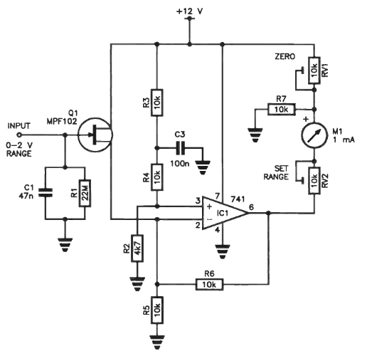
- IC1: 741 operational amplifier (signal processing)
- Q1: MPF102 JFET transistor (high impedance input buffer)
- M1: 1mA analog meter (visual display)
Understanding S-MeterCircuit Design
This simple S-meter circuit uses readily available components to create an effective signal strength indicator. The design centers around an op-amp 741 integrated circuit with supporting components for accurate measurement.
The active components include the IC1 741 operational amplifier for signal processing, Q1 MPF102 JFET transistor providing high impedance input buffering, and M1 1mA analog meter for visual display. The passive network consists of multiple 10k resistors creating the bias and feedback networks, along with R1 2.2M resistor for input bias, potentiometer R7 for zero adjustment, and variable resistors RV1 and RV2 for range control. Capacitors C1 47nF and C3 100nF handle input coupling and supply decoupling respectively.
How the S-Meter Circuit Works
The signal path begins when the 0-2V input signal enters through capacitor C1, which blocks DC components while allowing AC signals to pass through to the measurement circuit. The JFET transistor Q1 using the MPF102 device provides crucial high input impedance buffering, preventing any loading of the receiver’s AGC line while maintaining signal integrity.
The 741 op-amp then amplifies and conditions this buffered signal for proper meter deflection. The processed signal finally drives analog meter M1, providing clear visual indication of the received signal strength. This arrangement ensures accurate measurement without interfering with the receiver’s normal operation.
Calibration and Adjustment Controls
Zero adjustment through potentiometer R7 allows setting the meter to read zero with no input signal present. This compensates for any DC bias variations in the circuit and remains essential for maintaining accurate readings over time.
The range control system using variable resistors RV1 and RV2 provides flexibility in setting maximum meter deflection and adjusting sensitivity for different signal levels. RV1 primarily controls the maximum deflection point, while RV2 fine-tunes the sensitivity to match various receiver types and their AGC voltage ranges.
S-MeterCircuit Operation Principles
The MPF102 JFET serves as the critical input buffer stage, offering extremely high input impedance that prevents loading the receiver’s delicate AGC circuit. This device maintains low noise characteristics while providing stable operation across normal temperature ranges, ensuring consistent performance in typical operating environments.
The 741 op-amp provides stable signal conditioning with predictable amplification characteristics and minimal temperature-related drift. Its wide bandwidth capability handles various signal frequencies encountered in typical receiver applications, making this design versatile across different radio types.
Input components should be positioned close to the JFET transistor Q1 to minimize noise pickup and maintain the high input impedance characteristics.
Consider using a metal enclosure to provide RF shielding, especially when the S-meter will be integrated into existing receiver equipment. This prevents interference from strong local signals and maintains measurement accuracy.
Calibration Process
The calibration procedure begins with zero setting by disconnecting any input signal and adjusting R7 until the meter reads exactly zero. Verify this setting remains stable over several minutes to ensure proper DC bias conditions.
Range calibration involves applying a known reference voltage, typically 1V, to the input while adjusting RV1 and RV2 for the desired meter deflection. Test the response with various signal levels from 0.1V to 2V in regular steps to verify proportional meter response throughout the range. Fine-tune the adjustments if the linearity appears unsatisfactory.
S-Meter circuitIntegration with Radio Receivers
Most receivers provide an AGC line tap that offers the most common connection point for S-meter circuits. This connection provides a DC voltage that varies proportionally with received signal strength and is usually available as a test point or designated connection in receiver schematics.
Alternative connection methods include tapping the IF amplifier output, though this may require signal attenuation depending on the specific receiver design. Some receivers may need level shifting circuits if their AGC systems operate with negative voltages relative to ground.
Performance Characteristics and Accuracy
This circuit handles input signals from 0 to 2V DC with input impedance exceeding 1 megohm due to the JFET buffer stage. The 1mA full-scale meter provides good sensitivity while the +12V DC power requirement at approximately 10mA keeps power consumption reasonable.
The frequency response extends from DC to several MHz, making it suitable for most receiver applications. Temperature stability depends primarily on the 741 op-amp characteristics, which provide reasonable performance for amateur applications. Using precision 1% resistors for critical values improves overall accuracy.
This receiver S-meter circuit demonstrates practical analog measurement techniques using readily available components. The combination of 741 op-amp and MPF102 JFET provides reliable signal strength indication while maintaining the high input impedance necessary to avoid loading sensitive receiver circuits.
